Analysis of active crystal oscillator pinout: CMOS, LVCMOS, TTL, LVTTL, LVDS

Common crystal oscillator pinout are as follows:
1. CMOS
The original intention of this interface level standard is to be used between digital systems based on MOS tube structure composed of NMOS and PMOS.
For the digital circuit working under the CMOS interface standard, the standard power supply of the internal active crystal oscillator is 5V.
crystal oscillator pinout and input conditions are as follows:
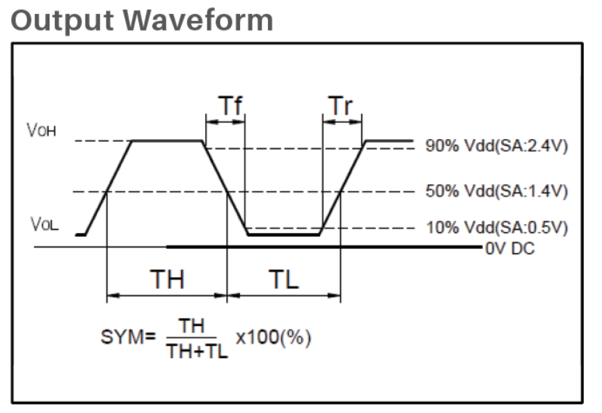
① For the output terminal, the voltage of state 1 is required to be greater than or equal to 4.45v,
and the voltage of state 0 is required to be less than or equal to 0.5V;
② For the input terminal, the determination requirement of state 1 is greater than or equal to 3.5V,
and the determination requirement of state 0 is less than or equal to 1.5V.
③ Compared with TTL interface, CMOS has greater noise tolerance, and its input impedance is much larger than TTL input impedance.
2. LVCMOS
LVCMOS is easier to communicate with lower voltage than LVTTL.
(1)LVCOMS3V3: the standard power supply of its internal active crystal oscillator is 3.3V, and the output and input conditions are as follows:
① For the output terminal, the voltage of state 1 is required to be greater than or equal to 3.2V, and the voltage of state 0 is required to be less than or equal to 0.4V;
② For the input terminal, the determination requirement of state 1 is greater than or equal to 2.0V, and the determination requirement of state 0 is less than or equal to 0.7V.
(2)LVCOMS2V5: the standard power supply of its internal active crystal oscillator is 2.5V, and the output and input conditions are as follows:
① For the output terminal, the voltage of state 1 is required to be greater than or equal to 2.0V, and the voltage of state 0 is required to be less than or equal to 0.4V;
② For the input terminal, the determination requirement of state 1 is greater than or equal to 1.7V, and the determination requirement of state 0 is less than or equal to 0.7V.
(3)LVCOMS1v8: the standard power supply of its internal active crystal oscillator is VCC = 1.8V. The introduction is as follows:
① For the output terminal, the voltage of state 1 is required to be greater than or equal to VCC-0.45v (if VCC is accurately equal to 1.8V, it is 1.35V),
and the voltage of state 0 is required to be less than or equal to 0.45V;
② For the input terminal, the determination of state 1 requires a VCC greater than or equal to 0.65 times (If VCC is exactly equal to 1.8V, it is 1.17v),
and the determination of state 0 requires a VCC less than or equal to 0.35 times ( if the VCC is accurately equal to 1.8V, it is 1.65V).
(4)LVCOMS1V5: the standard power supply of its internal active crystal oscillator is VCC = 1.5V, and its tolerance will affect its output and input, as described below:
① For the output terminal, LVCOMS1V5 has no specific requirements, but it must be that the closer state 1 is to VCC, the better, and the closer state 0 is to 0V;
② For the input terminal, the determination of state 1 requires VCC greater than or equal to 0.65 times (if VCC is accurately equal to 1.5V, it is 0.975V),
and the determination of state 0 requires VCC less than or equal to 0.35 times ( if VCC is accurately equal to 1.5V, it is 0.525V).
(5)LVCOMS1V2:the standard power supply of its internal active crystal oscillator is VCC = 1.2V, and its tolerance will also affect its output and input, as described below:
① For the output terminal, LVCOMS1V2 has no clear requirements, but it must be that the closer state 1 is to VCC, the better, and the closer state 0 is to 0V;
② For the input terminal, the determination of state 1 requires VCC greater than or equal to 0.65 times ( if VCC is accurately equal to 1.2V it is 0.78V),
and the determination of state 0 requires VCC less than or equal to 0.35 times (if VCC is accurately equal to 1.2V, it is 0.42V).
3. TTL
The original intention of this interface level standard is to be used for the interface between digital systems based on triode structure.
For digital circuits operating under TTL interface standard, the standard power supply of internal active crystal oscillator shall be 5V,
and the crystal oscillator pinout and input conditions are as follows:
① For the output terminal, the voltage of state 1 is required to be greater than or equal to 2.4V, and the voltage of state 0 is required to be less than or equal to 0.5V;
② For the input terminal, the determination requirement of state 1 is greater than or equal to 2.0V, and the determination requirement of state 0 is less than or equal to 0.8V.
③ That is, it needs to be greater than a certain threshold to represent level 1, and less than a certain threshold to represent level 0.
Comparing the voltage requirements of the output and input terminals,
it can be seen that the voltage output requirements of the output terminal are more stringent than the double threshold judgment standard of the input terminal.
This mainly takes into account the interference of noise and the transmission speed of electrical signals between output and input,
so as to make the double threshold judgment standard more reliable.
4. LVTTL
Because there is still a large space between 2.4V and 5V, it has no obvious benefit to improve noise interference,
and it will increase the power consumption of the system. In addition, due to the large level difference between digital states 1 and 0,
the response speed of digital circuit will be affected. Therefore, the voltage range of TTL was compressed to form a low-voltage TTL level standard.
(1)LVTTL3V3: the standard power supply of its internal active crystal oscillator is 3.3V. The output and input conditions are as follows:
For the output terminal, the voltage of state 1 is required to be greater than or equal to 2.4V, and the voltage of state 0 is required to be less than or equal to 0.4V;
For the input terminal, the determination requirement of state 1 is greater than or equal to 2.0V, and the determination requirement of state 0 is less than or equal to 0.8V.
Comparing the voltage requirements of the output and input terminals,
it can be seen that in order to ensure the stability and noise resistance of the double threshold judgment,
the voltage requirements of the output terminal are still stricter than the double threshold judgment standard of the input terminal.
This is the same for all digital system interface standards.
(2)LVTTL2V5:the standard power supply of its internal active crystal oscillator is 2.5V. The output and input conditions are as follows:
① For the output terminal, the voltage of state 1 is required to be greater than or equal to 2.0V, and the voltage of state 0 is required to be less than or equal to 0.2V;
② For the input terminal, the determination requirement of state 1 is greater than or equal to 1.7V, and the determination requirement of state 0 is less than or equal to 0.7V.
5. LVDS
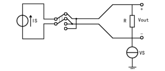
LVDS is low-voltage differential signal. Its input and output are different from the interface level introduced earlier.
It needs to complete communication through two lines. Its working principle is shown in the figure below:

PS:
It is recommended to select a consistent standard for both sides of the digital system interface.
For example, in the selection of active crystal oscillator, special attention should be paid to the crystal oscillator pinout in the crystal oscillator specification.
In addition, single ended and differential are not compatible because they are different in physical connection.
However, for the same kind of interface, if the output of level A standard meet the input of level B standard,
it is said that the output of level A can drive the input of level B. If vice versa, it is said that the two level standards of level A and B can drive each other.
For example, the output of CMOS can drive the TTL input, but vice versa, because the output of TTL state 1 is only greater than or equal to 2.4V,
which can not reach the 3.5V required by CMOS decision state 1. However,LVTTL3v3 and LVCMOS3v3 can drive each other,
because their outputs can meet each other's input judgment requirements.
