CMOS oscillator introduction | Xtalong
The crystal oscillator is just a general term, which could be divided into passive crystal oscillator and active crystal oscillator.
The passive crystal output waveform is generally sine wave while SPXO is a CMOS oscillator,
which is the most common one of square wave output. So below we will continue to explain how CMOS oscillator circuit design works.
CMOS oscillator circuit design
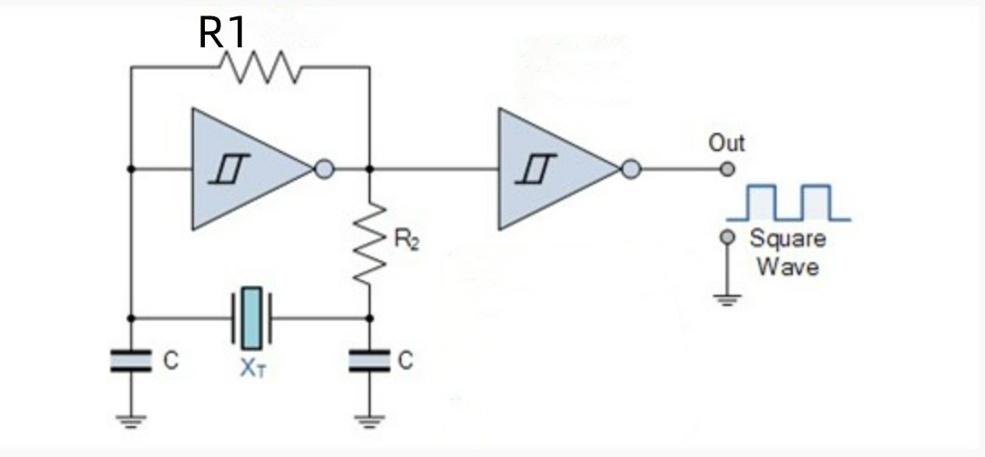
The CMOS inverter is initially biased to the middle of its working area through the feedback resistor R1.
This ensures that the Q-point of the inverter is in the high gain region. A resistance of 1mΩis used here,
but its value is not important as long as it is above 1MΩ.
An additional inverter is used to buffer the output of the oscillator to the connected load.
The inverter provides a 180 ° phase shift, and the crystal oscillator capacitor network requires an additional 180 ° oscillation.
The advantage of the CMOS oscillator is that it will always automatically readjust to maintain the 360 ° phase shift of the oscillation.

How CMOS oscillator circuit worked?
Unlike the transistor-based crystal oscillator that previously generated sinusoidal output waveform,
because the CMOS inverter oscillator uses a digital logic gate, the output is a square wave oscillating between high and low.
Of course, the maximum operating frequency depends on the switching characteristics of the logic gate used.
below link is our SMD CMOS oscillator details :
