Email: sales@xtalong.com Tel: +86-28-80192520
Email: sales@xtalong.com Tel: +86-28-80192520
Frequency: 25MHz
Supply Voltage(Vcc): 1.8V/2.8V/3.0V
Frequency Stability Vs Temperature: ±0.05ppm/℃ max.(-30 ~ +85℃)
Initial Frequency Tolerance: ±2.0ppm max.
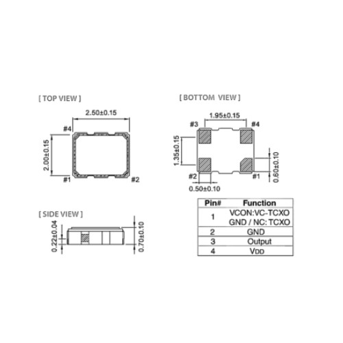
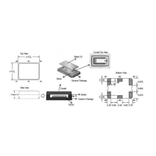
25MHz SMD 2520 TCXO – Ultra-Compact High Stability Reference Clock
Product Overview:
The 25MHz TCXO in the SMD 2520 (2.5mm x 2.0mm) package is designed for space-constrained applications requiring superior frequency stability. Delivering ±0.5ppm precision across an extended temperature range, this oscillator features a Cliped Sine Wave output for reduced EMI. With a remarkably low current draw of only 1.5mA, it is the perfect timing solution for battery-powered devices, GPS/GNSS receivers, and modern telecommunication systems.
Key Features:
Ultra-Small Footprint: Compact 2.5 x 2.0 mm SMD package saves critical PCB real estate.
High Frequency Stability: Offers tight ±0.5ppm stability from -30°C to +85°C.
Low Phase Noise: Excellent performance with -130 dBc/Hz at 1kHz offset, ensuring high signal integrity.
Extreme Low Power: Consumes maximum 1.5mA, extending battery life in portable applications.
Wide Supply Voltage: Flexible operation from +1.7V to +3.3V.
Fast Start-up: Rapid initialization in less than 2ms.
EMI Optimized: Cliped Sine Wave output minimizes electromagnetic interference.
Ideal Applications:
GPS / GNSS Modules: High-precision reference for positioning and navigation systems.
Mobile Communications: Smartphones, wearables, and portable radio equipment.
IoT Devices: Low-power timing for smart sensors and connected devices.
Wireless Connectivity: Wi-Fi, Bluetooth, and cellular backhaul.
Model | TCXO SMD252025Mhz 3.3V |
| Size | SMD2520 |
| Frequency | 25 MHz |
| Type | TCX0 |
Vcc | +1.7V~+3.3V |
Vcount | N/A |
| AFC Range. | N/A |
| Temp | ±0.5ppm max.@-30~+85℃ |
| Slope | ±0.05ppm/℃ max.@-20~+65℃ |
| Initial Frequency | ±2.0ppm max. (After 2times reflow) |
| Parameter | Value | Conditions | |
| Frequency | 25.000000MHz | ||
| Supply VoltagelVcc | +1.8±5%,+2.8V±5%,+3.0±5% | ||
| Output Load | 10kohm//10pF±10% | ||
| Control Voltage[Vcont | NA | ||
| Output Level | 0.8Vp-pmin | Cliped sine wave (DC-coupled) | |
| Current | .5mAmax. | 0koms//10pF±10% | |
| Duty Cycle | 50±5% | ||
| Operating Temperature Range | 40~+85℃ | ||
| Storage Temperature Range | 40~+85℃ | ||
| Initial Frequency Tolerance | ±2.0ppm max | After 2times reflow | |
| FrequencyStability | Vs.Temperature(-30~+85℃) | ±0.5ppm max | Referenced to+25℃ frequenc |
| vs.Temperature (-40~-30℃) | ±3.0ppm max. | ||
| vs.Supply Voltage | ±0.2ppm max. | Vcc±5% | |
| Vs.Load | ±0.2ppm max. | 10koms//10pF±10%each | |
| Vs.Aging | ±1.0ppm max. | 1st Year | |
| Frequency Slope | Vs.Temperature(.20~+65℃) | ±0.05ppm/C max | Every+2℃ |
| vs.Temperature (-30~+85℃) | ±0.1ppm/℃ max | ||
| vs.Temperature(-40~-30℃) | ±0.35pom/℃ max | ||
| Start.up Time | 2ms max | Morethan 90%offinal amplitude | |
| Phase Noise | -130dBcHz max | 1KHz offset | |


Notes:
- Please connect a bypass capacitor closely to Vcc Pad.
- Load capacitance (CL) includes probe and test board capacitance


Contact: Katya Vane
Phone: +86-18884136031
Tel: +86-28-80192520
Email: sales@xtalong.com
Add: No.4 of XinHang Road, West of High-tech zone, Chengdu City 611731, China
We chat