Email: sales@xtalong.com Tel: +86-28-80192520
Email: sales@xtalong.com Tel: +86-28-80192520
Frequency: 20MHz
Frequency Tolerance: ±1ppm
Frequency Stability: ±0.28ppm
Operating Supply Voltage Range: 3.135V ~ 3.465V
20MHz High-Precision TCXO (±0.28ppm, Clipped Sine Wave, 5.0x3.2mm)
Product Overview
The 20MHz TCXO is a high-stability Temperature Compensated Crystal Oscillator designed for mission-critical timing. Housed in a robust 5.0x3.2mm (5032) 10-pad ceramic package, it offers a superior ±0.28ppm stability across an industrial temperature range of -40°C to +85°C.
With its clipped sine wave output, this oscillator ensures reduced power consumption (only 3.5mA) and minimized harmonic distortion, making it an ideal choice for GPS/GNSS receivers, handheld IoT devices, and high-accuracy laboratory instruments.
Key Highlights
High Precision: ±0.28ppm stability ensures reliable synchronization in GNSS applications.
Low Power Consumption: Typ. 3.5mA, extending battery life for portable IoT devices.
Phase Noise Excellence: -155 dBc/Hz @ 100kHz offset for superior signal integrity.
Industrial Reliability: Operates flawlessly from -40°C to +85°C.
Specialized Design: 10-pad configuration for enhanced grounding and stability.
1. NOMINAL AND MAXIMUM RATINGS, OPERATING AND STORAGE CONDITIONS
| Item | Parameters | Symb. | Min. | Typ. | Max. | Unit | Conditions /Remarks |
1 | Nominal frequency | FN | 20.000 | MHz | |||
2 | Maximum supply voltage | VMax. | -0.3 | +4.0 | VDC | Between VCC and GND | |
3 | Operating Supply Voltage Range | Vcc | 3.135 | 3.30 | 3.465 | VDC | |
4 | Output Load Resistance | RL | 9 | 10 | 11 | kΩ | Clipped sine wave output |
5 | Output Load Capacitance | CL | 9 | 10 | 11 | pF | Clipped sine wave output |
6 | Operating Temperature Range | ToP | -40 | +25 | +85 | ℃ | Note 1 |
7 | Storage Temperature Range | TsT | -40 | +85 | ℃ | ||
Note 1: over the whole range, the unit stays within all relevant parameter limits as specified under point 2
2. ELECTRICAL PARAMETER LIMITS
Parameters | Symb. | Min. | Typ. | Max. | Unit | Conditions /Remarks | |
1 | Frequency Tolerance | △f/FN | -1.0 | +1.0 | ppm | Offset from nominal at +25°℃ | |
2 | Frequency Stability | △f/FRFL | -0.28 | +0.28 | ppm | Note 1 | |
3 | Frequency VS Voltage Changes | △f/FV | -0.1 | +0.1 | ppm | Vcc±5% at +25℃ | |
4 | Frequency VS Load Changes | △f/FL | -0.1 | +0.1 | ppm | ||
5 | Aging 20 years | △f/FA1 | -3.0 | +3.0 | ppm | at +25℃ | |
6 | Output Amplitude Voltage Level | VP-P | 0.8 | VAC | Clipped sine wave | ||
7 | Output Symmetry (Duty Cycle) | DC | 45 | 55 | % | GND level (DC cut) | |
8 |
|
| -98 |
| at 10Hz offset /at +25℃ | ||
-125 | at 100Hz offset/at+25℃ | ||||||
-145 | at 1kHz offset /at +25℃ | ||||||
-150 | at 10kHz offset /at +25℃ | ||||||
-155 | at 100KHz offset /at+25℃ | ||||||
9 | Startup Time | tSTRT | 2.0 | ms | Vp-p reach > 90% of amplitude | ||
10 | Current Consumption | ICC | 3.5 | mA |
Note 1:Frequency stability is the frequency deviation over operating temperature range TOP in reference to the frequency reading at +25°C.
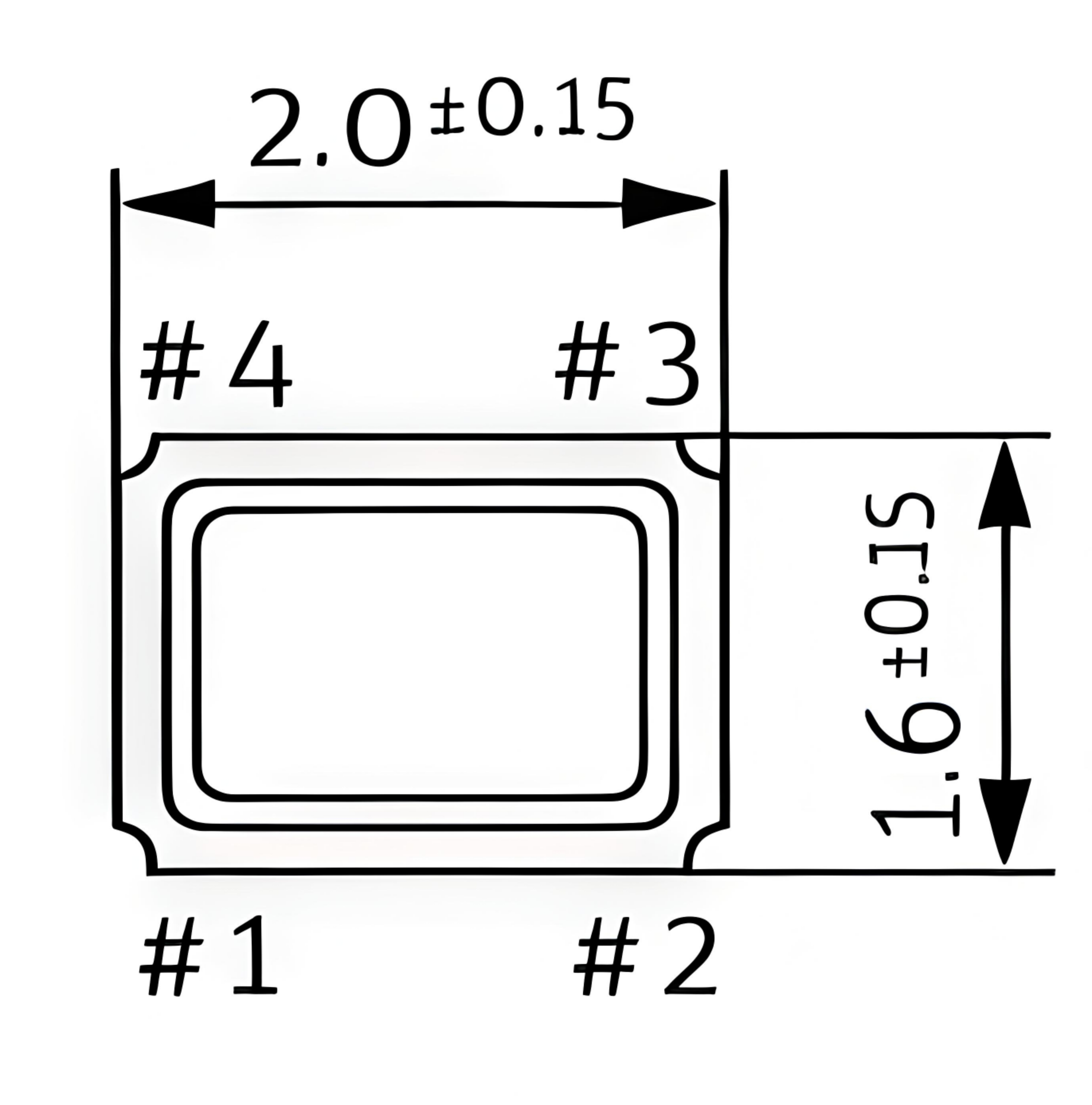
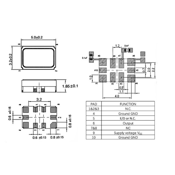
3.OUTLINE DRAWING
Package description
Ceramic seam seal SMD package 5.0x3.2mm with 10 pads

RECOMMENDED SOLDERING INFORMATION

PACKAGING

Contact: Katya Vane
Phone: +86-18884136031
Tel: +86-28-80192520
Email: sales@xtalong.com
Add: No.4 of XinHang Road, West of High-tech zone, Chengdu City 611731, China
We chat