Email: sales@xtalong.com Tel: +86-28-80192520
Email: sales@xtalong.com Tel: +86-28-80192520
Nominal Frequency: 26MHz
Frequency Stability: ±0.5ppm @ -30~85℃
Operating Temperature Range: -40~85℃
Aging: ±1ppm
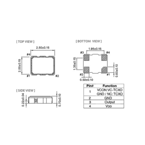
26.000 MHz VCTCXO - SMD 2520 (±0.5ppm, Clipped Sine Wave)
The 26MHz VCTCXO (Voltage Controlled Temperature Compensated Crystal Oscillator) is engineered for ultra-high stability and precision. Housed in a miniature 2520 SMD package (2.5mm x 2.0mm), it delivers exceptional ±0.5ppm frequency stability over an extended temperature range of -30°C to +85°C (and operational up to -40°C).
This high-performance oscillator is optimized for GPS/GNSS, telecommunications, and wireless communication systems that require a low-jitter, stable clock source with a Clipped Sine Wave output.
Key Features:
Frequency: 26.000000 MHz
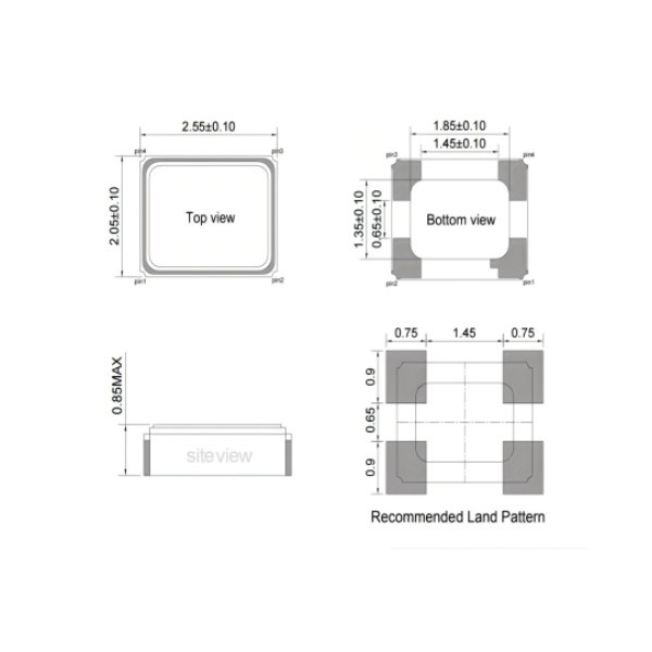
Package Size: Compact 2.5 x 2.0 x 0.9 mm (2520 SMD)
Ultra-High Stability: ±0.5ppm from -30°C to +85°C
Low Phase Noise: -138 dBc/Hz @ 1kHz offset
Output Type: Clipped Sine Wave for reduced EMI
Low Power Consumption: Max 2.0 mA
Voltage Control: Integrated Vcon for frequency tuning
Applications:
GPS / GNSS / Navigational Systems
5G / LTE Telecommunication Infrastructure
Smartphones and Portable Devices
IoT / Wireless Sensor Networks
Smart Grids and Industrial Automation
| ltem | Parameters | Condition | Electrical Specifications | ||||
| Min | Typ | Max | Units | ||||
| 1 | Nominal Frequency | 26.000000 | MHz | ||||
| 2 | Frequency Stability | Vs.Temperature (Note1) | @-40℃~-30℃ | -2.0 | 2.0 | ppm | |
| @-30℃~85℃ | -0.5 | 0.5 | ppm | ||||
| 3 | Vs.Load | ±10% | -0.2 | 0.2 | ppm | ||
| 4 | Vs.Supply Voltage | Standard Vcc±5% | -0.2 | 0.2 | ppm | ||
| 5 | Operating Temperature Range | -40 | 85 | ℃ | |||
| 6 | Frequency Tolerance | (Note2) | -2.0 | 2.0 | ppm | ||
| 7 | Supply Voltage | (Note3) | 2.66 | 2.80 | 2.94 | V | |
| 8 | Current Consumption | 2.0 | mA | ||||
| 9 | Output Level | (Note4) | 0.8 | Vp-p | |||
| 10 | Output Waveform | Clipped Sine | |||||
| 11 | Output Load | 10kΩ //10pF | |||||
| 12 | Duty Cycle | 40 | 50 | 60 | % | ||
| 13 | Control Voltage Range | 0.4 | 1.4 | 2.4 | V | ||
| 14 | Frequency Control Range (refer:Vcon=1.4V) | Vcon=0.4V | -15 | -9 | ppm | ||
| Vcon=2.4V | 9 | 15 | ppm | ||||
| 15 | Input Impedance | 500 | kΩ | ||||
| 16 | Aging | 1st year@25℃ | -1.0 | 1.0 | ppm | ||
| 17 | Phase Noise | @10 Hz offset | -94 | dBc/Hz | |||
| @100 Hz offset | -119 | dBc/Hz | |||||
| @1 kHz offset | -138 | dBc/Hz | |||||
| @10 kHz offset | -148 | dBc/Hz | |||||
| @100 kHz offset | -153 | dBc/Hz | |||||
| @1 MHz offset | -154 | dBc/Hz | |||||
| 18 | Start-up Time | To 90%of Vp-p | 2.0 | ms | |||
| 19 | Storage Temperature | -40 | 85 | ℃ | |||
Note1 Referenced to the midpoint between minimum and maximum frequency value
Note2 Refer to nominal frequency
Note3 Selectable operating voltage range:1.7~3.6V,electrical parameters measured under typical supply voltage
Note4 DC-cut capacitor of output is not put in TCXO.Please add DC-cut capacitor (above 1nF)in output line

| Name | Connection |
| Pin 1 | Vcon |
| Pin 2 | GND |
| Pin 3 | Fout |
| Pin 4 | Vcc |
Contact: Katya Vane
Phone: +86-18884136031
Tel: +86-28-80192520
Email: sales@xtalong.com
Add: No.4 of XinHang Road, West of High-tech zone, Chengdu City 611731, China
We chat