Email: sales@xtalong.com Tel: +86-28-80192520
Email: sales@xtalong.com Tel: +86-28-80192520
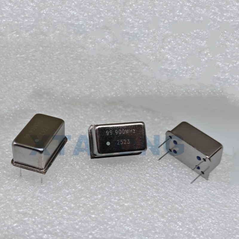
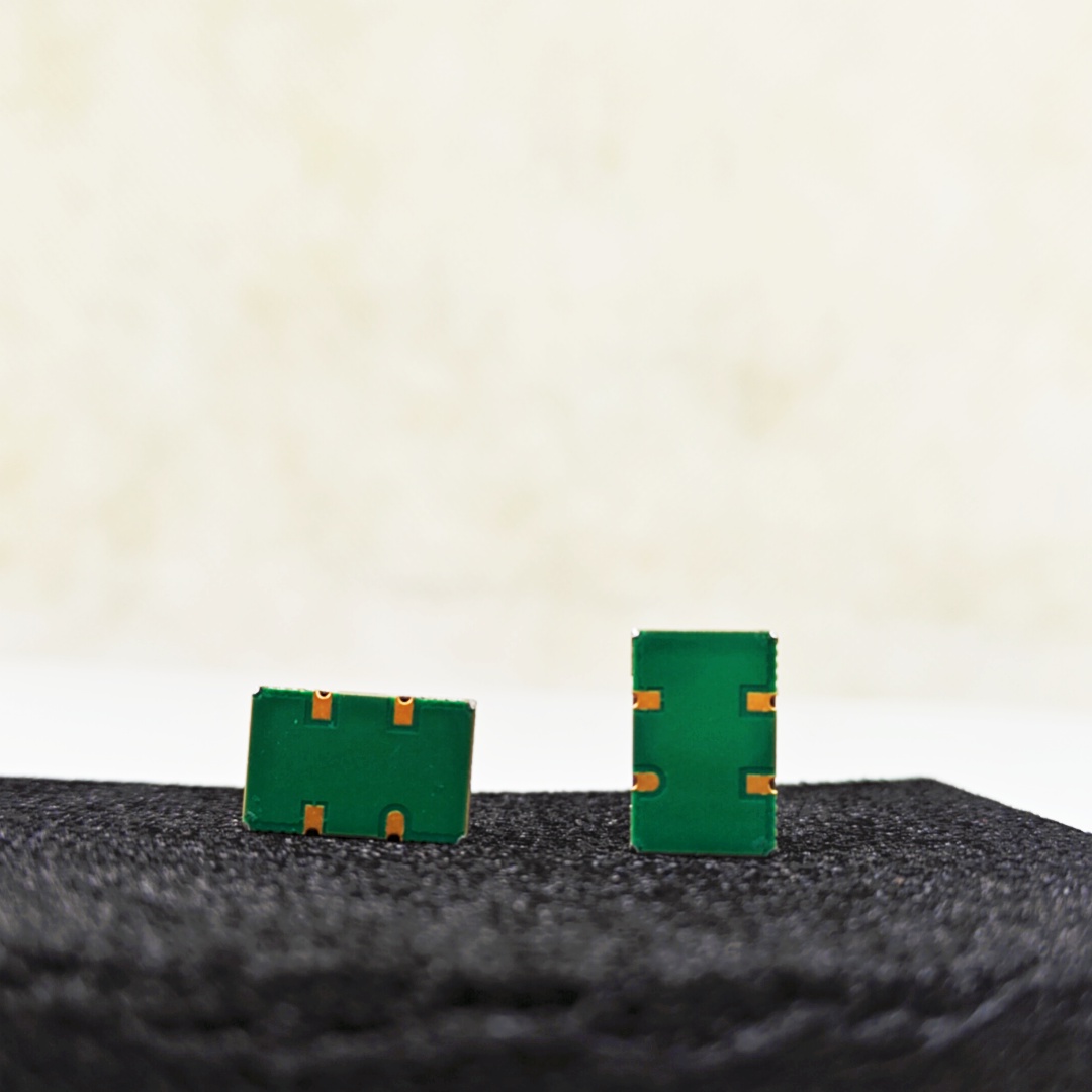
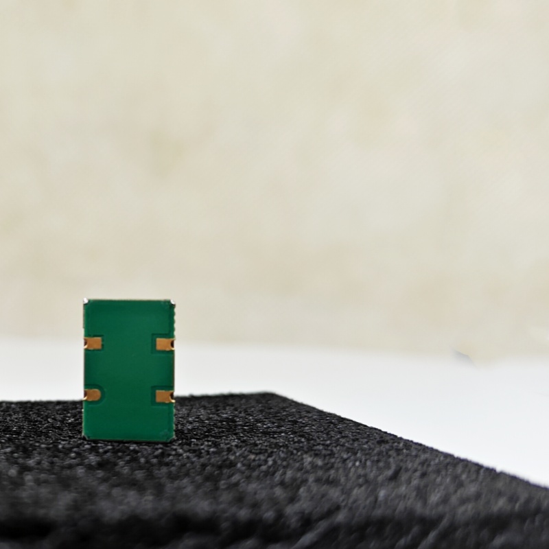
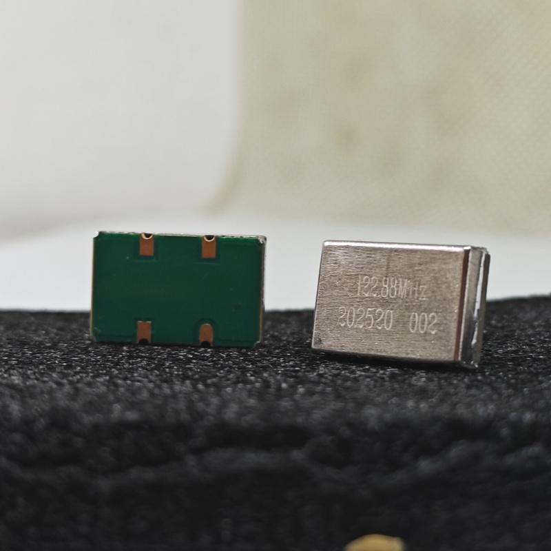
VCXO 99.9MHz DIP 14 package, Voltage Controlled Oscillator Design at 99.9 MHz
Voltage Controlled Oscillator Design at 99.9 MHz
Discover our advanced voltage-controlled oscillator (VCXO) design tailored for optimal performance at 99.9 MHz. This innovative VCXO design features enhanced stability, low phase noise, and efficient power consumption, making it ideal for a variety of applications in telecommunications and signal processing. Our expertise in voltage-controlled oscillator design ensures reliable and precise frequency control, meeting the demands of modern electronic systems. Explore the benefits of our cutting-edge VCXO solutions today!
Main data:
| Item | Min | Typ. | Max | Unit | Conditions | ||||||||||||||||||||
| Nominal frequency | 99.900 | MHz | -- | ||||||||||||||||||||||
| Frequency tolerance | –10 | +10 | ppm | Offset from FN at +25°C | |||||||||||||||||||||
| Frequency stability (overall) | –35 | +35 | ppm | Note 1 | |||||||||||||||||||||
| Aging first year | –3.0 | +3.0 | ppm | at +25°C | |||||||||||||||||||||
| Frequency pulling | ±50 | ppm | Min. over control volt. range | ||||||||||||||||||||||
| Linearity of frequency pulling | 10 | % | |||||||||||||||||||||||
| Modulation bandwidth | 10 | kHz | Measured at 3dB | ||||||||||||||||||||||
| Output level | +5 | dBm | |||||||||||||||||||||||
| Harmonic | -30 | dBc | |||||||||||||||||||||||
| Spurious | -70 | dBc | |||||||||||||||||||||||
| Phase noise | -130 | dBc/Hz | at 10kHz | ||||||||||||||||||||||
| Phase Jitter RMS | 1.0 | ps | At 12kHz~20MHz / +25°C | ||||||||||||||||||||||
| Current consumption | 40 | mA | With output load CL ±10% | ||||||||||||||||||||||
| Startup time | 10 | ms | VP-P reach >90% of amplitude | ||||||||||||||||||||||
| Maximum voltage range | –0.5 | +7.0 | VDC | Between VCC and GND | |||||||||||||||||||||
| Operating supply voltage | 4.5 | 5.0 | 5.5 | VDC | -- | ||||||||||||||||||||
| Control voltage range / center | 0 | 2.5 | 5.0 | VDC | Pin 1 | ||||||||||||||||||||
| Control voltage input impedance | 100 | kΩ | Pin 1 | ||||||||||||||||||||||
| Output load | 50 | Ω | Sine Wave | ||||||||||||||||||||||
| Operating temperature range | 0 | +25 | +70 | °C | -- | ||||||||||||||||||||
| Storage temperature range | –55 | +125 | °C | -- | |||||||||||||||||||||

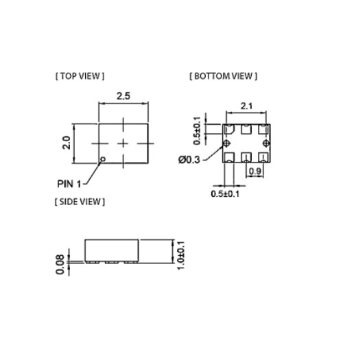
Pin function:
| Pin Number | Function |
| #1 | Voltage control |
| #7 | Ground |
| #8 | RF output |
| #14 | Voltage input |
Frequency: 99.9MHz (±10ppm tolerance)
Phase Noise: -130dBc/Hz @10kHz for minimal signal distortion
Voltage Control: Adjustable tuning for fine frequency calibration
Output Type: CMOS/LVCMOS (configurable)
Temperature Stability: ±5ppm over operating range
Supply Voltage: 3.3V or 5V (customizable)
Package Options: SMD or through-hole (as per requirement)
Precision Test & Measurement Equipment
Wireless Communication Systems
Radar & Satellite Technology
Medical & Scientific Instruments
Custom Clock Distribution Networks
This custom 99.9MHz VCO is designed for applications demanding ultra-tight frequency control and low phase noise. Whether for prototyping or production, we provide tailored voltage controlled oscillator designs to meet exact performance requirements.
Contact: Katya Vane
Phone: +86-18884136031
Tel: +86-28-80192520
Email: sales@xtalong.com
Add: No.4 of XinHang Road, West of High-tech zone, Chengdu City 611731, China
We chat