Email: sales@xtalong.com Tel: +86-28-80192520
Email: sales@xtalong.com Tel: +86-28-80192520
Frequency: 10MHz
Supply Voltage: 12 V
Output level: Sine wave
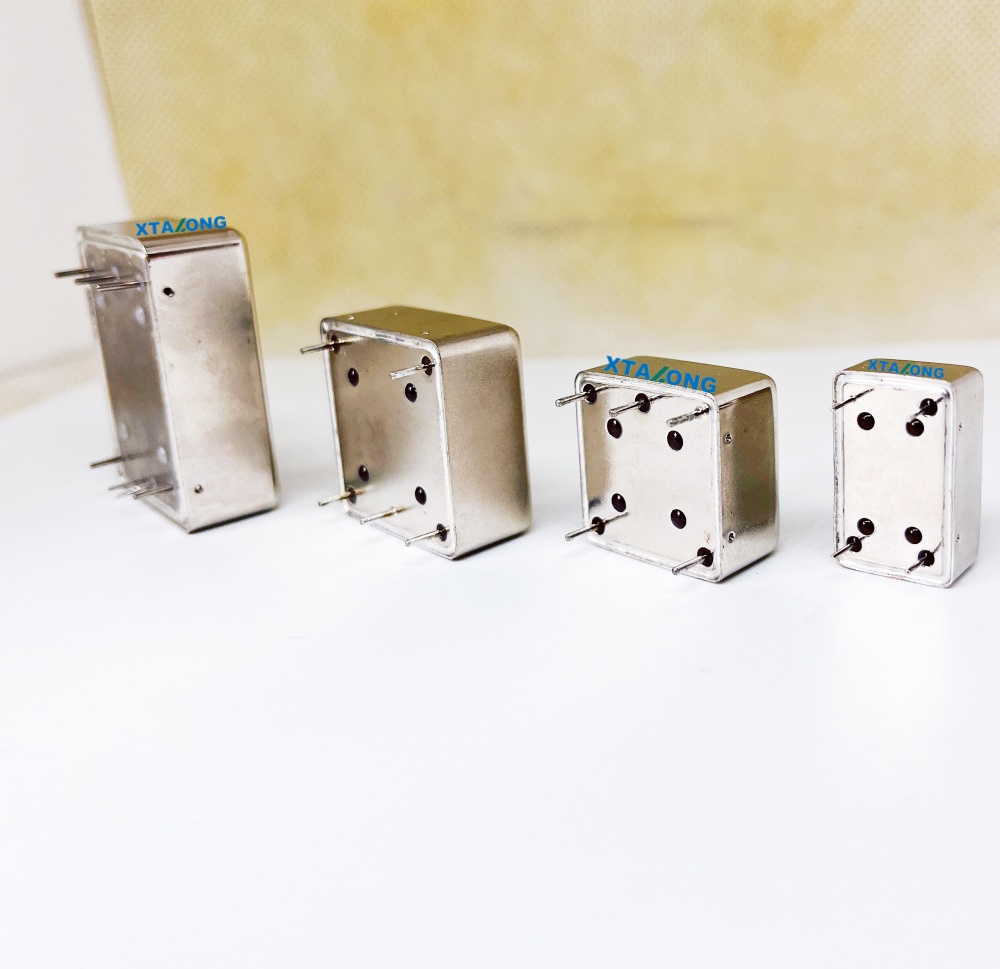
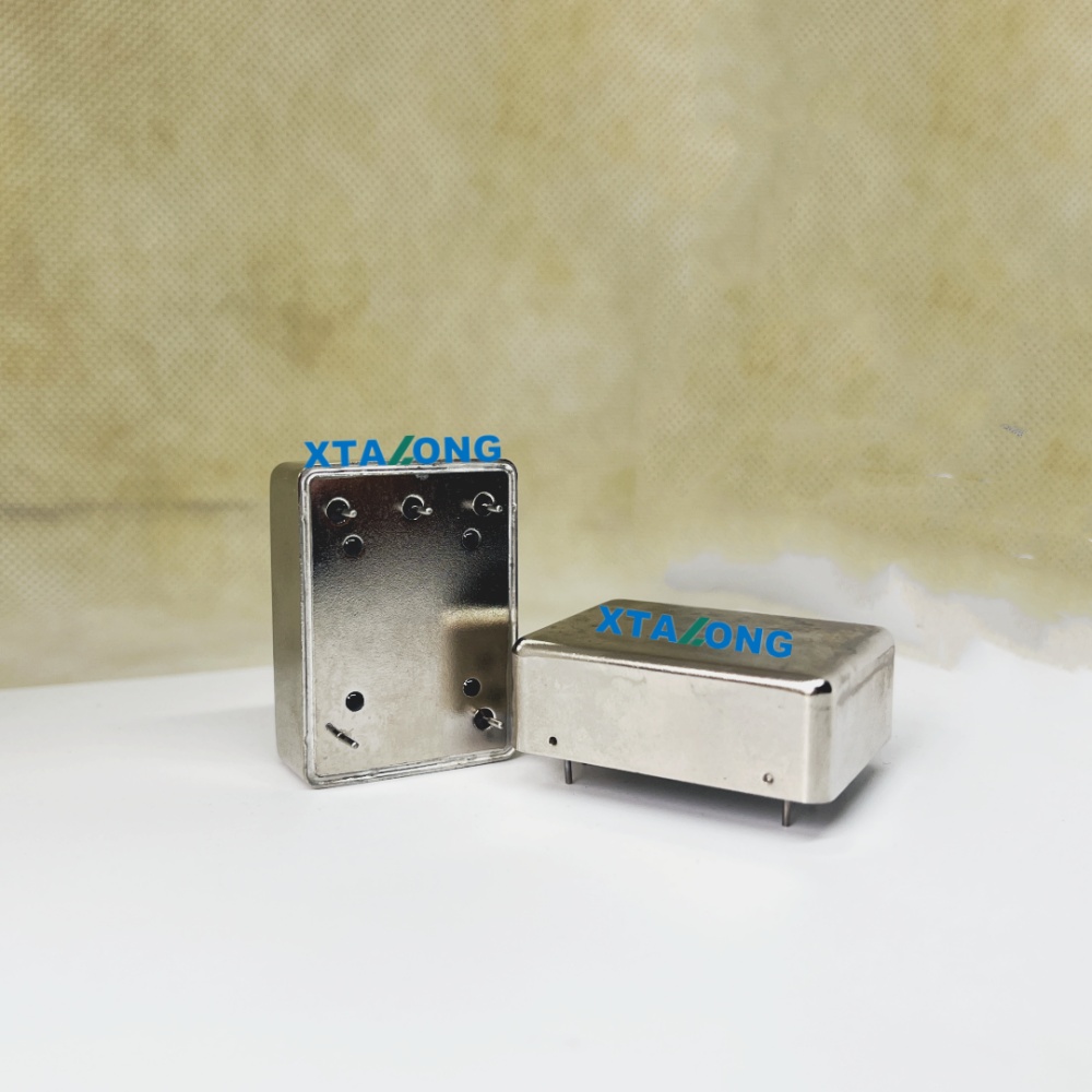
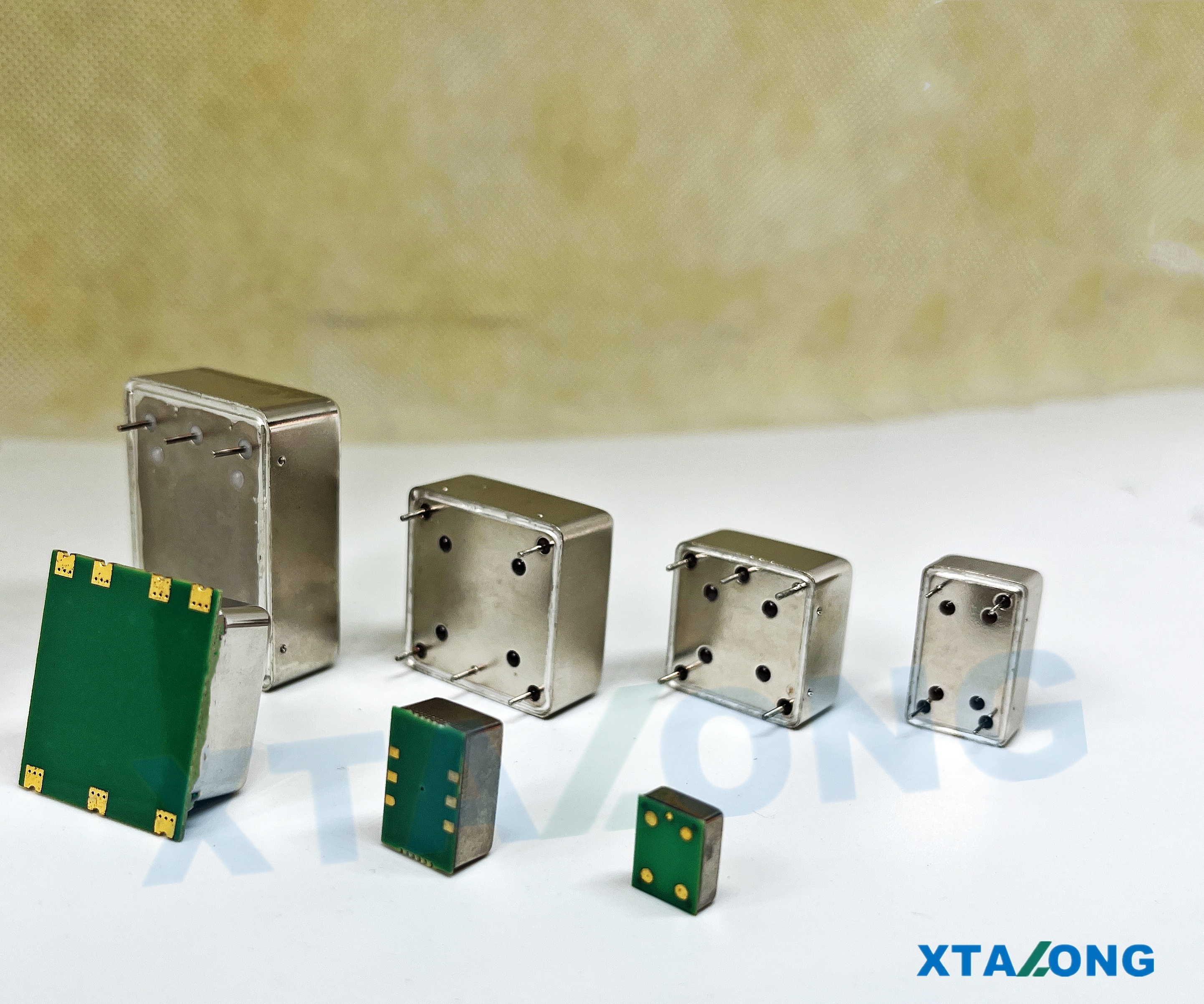
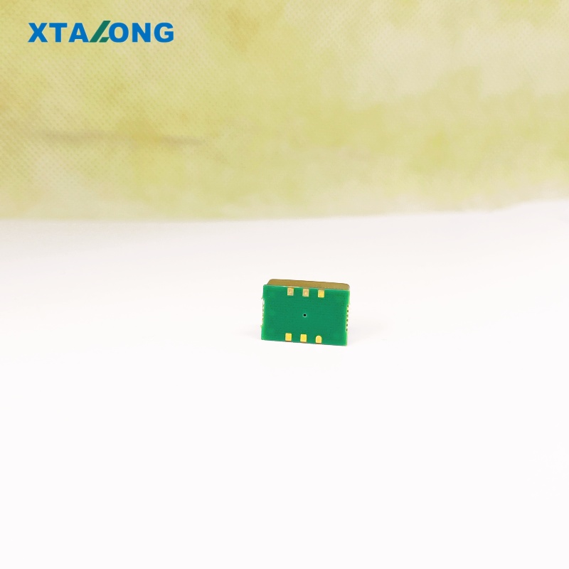
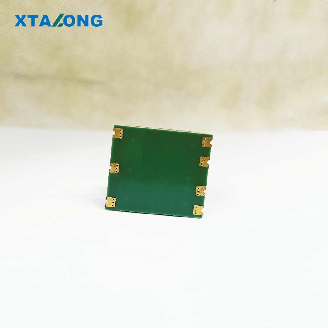
Package Size: 25.4 x 22 x 13.20 mm
Ultra Low Phase Noise 10MHz SMD OCXO – High Precision Reference
Product Overview:
Our 10MHz OCXO is a high-performance, oven-controlled Crystal Oscillator housed in a compact SMD package. Designed for mission-critical applications, it offers ultra-low phase noise performance (up to -115 dBc/Hz at 1Hz offset) and exceptional short-term stability (Allan Variance of 0.002 ppb). This series features an integrated electrical frequency tuning input and a reference voltage output, making it easy to integrate into complex microwave systems.
Key Features:
Ultra-Low Phase Noise: Multiple options available, reaching -115 dBc/Hz @ 1Hz and a noise floor of -170 dBc/Hz.
Compact SMD Design: Ideal for space-constrained PCB layouts without sacrificing stability.
Exceptional Stability: Tight frequency stability options from ±5 ppb to ±100 ppb.
Superior Allan Variance: 0.002 ppb (t=1 sec), ensuring ultra-precise short-term timing.
Fast Warm-up Time: Reaches stability within 5 minutes at 25°C.
Rugged Construction: Built to meet MIL-STD-202 standards for vibration and shock.
Easy Integration: Includes Electrical Frequency Tuning (VCO Input) and Reference Voltage Output.
Applications:
Radar Systems: Low phase noise ensures superior target detection and signal clarity.
Test & Measurement: High-stability reference for frequency counters and synthesizers.
Microwave Communication: Critical for clock references in microwave signal sources.
Telecom Systems: Reliable synchronization for high-speed data networks.
Test conditions: VDC = +12 V; VCO = +5 V; at +25 ± 3°C unless otherwise identified
| Parameter | Min. | Typ. | Max. | Unit | Test Condition |
| Frequency | 10 | MHz | |||
| Initial Accuracy | -0.1 | 0.1 | ppm | @+25±1℃ | |
| after turn on power 60 minutes | |||||
| Vco=+5V | |||||
| Waveform | Sine wave | ||||
| Level | 8 | 10 | 12 | dBm | |
| Load | 50 | ||||
| Harmonics | -30 | dBc | |||
| Spurious | -80 | dBc | 10Hz to 1MHz from carrier | ||
| 2.Frequency Stability | |||||
| Parameter | Min. | Typ. | Max. | Unit | Test Condition |
| Ambient | ±5,±10,±20,±30,±50,±100 | ppb | referenced to 25℃ | ||
| -20℃~+70℃ | ℃ | ||||
| -40℃~+85℃ | |||||
| Aging | |||||
| Daily | -0.5 | 0.5 | ppb | after 30 days of continuous operation | |
| Yearly | -50 | 50 | ppb | ||
| 10 Years | -0.3 | 0.3 | ppm | ||
| Voltage | -1 | 1 | ppb | ±5%change | |
| Short term | 0.002 | ppb | root Allan variance for t=1 sec | ||
| Load | -1 | 1 | ppb | ±5%change | |
| Warm-up | -50 | 50 | ppb | in 5minutes @+25±1 referenced to 1 hour | |
| Phase Noise (Max. ) | Option 1 | Option 2 | Option 3 | ||
| -105 | -110 | -115 | dBc/Hz | @1Hz | |
| -135 | -140 | -142 | dBc/Hz | @10Hz | |
| -155 | -155 | -155 | dBc/Hz | @100Hz | |
| -165 | -165 | -165 | dBc/Hz | @1KHz | |
| -170 | -170 | -170 | dBc/Hz | @10KHz | |
| -170 | -170 | -170 | dBc/Hz | @100KHz | |
| 3.Electrical Frequency Adjustment(PIN=“VCO INPUT”) | ||||||
| Parameter | Min. | Typ. | Max. | Unit | Test Condition | |
| Tuning Range | ±0.4* | ppm | Referenced to frequency at nominal Center Voltage | |||
| Control | 0.5 | 9.5 | V | |||
| Slope | Positive | |||||
| Center | 5 | V | ||||
| Linearity | -10 | 10 | % | |||
| 4.Input Power(PIN=“+VDC”) | ||||||
| Parameter | Min. | TyP. | Max. | Unit | Test Condition | |
| Voltage | 11.4 | 12 | 12.6 | V | ||
| Current | ||||||
| Steady State | 2 | W | @+25℃,operating-20℃~+70℃ | |||
| 2.3 | @+25℃,operating-40C~+85℃ | |||||
| During Warm-Up | 400 | mA | @+25℃,operating-20℃~+70℃ | |||
| 500 | @+25℃,operating-40℃~+85℃ | |||||
| 5.Reference Voltage(PIN="REFERENCE VOLTAGE") | ||||||
| Parameter | Min. | Typ. | Max | Units | Test Condition | |
| Voltage | 9.25 | 9.5 | 9.75 | V | ||
| Source | 100 | Ohm | ||||
| Load | 10 | Kohm | ||||
| 6.Environental | ||||||
| Parameter | Reference Std. | Test Condition | ||||
| Operable Temperature | -45℃ to+90℃ | |||||
| Storage Temperature | -50℃ to+95℃ | |||||
| Humidity | MIL-STD-202,Method 103 | 95%RH @+40℃,non- condensing.240 hours | ||||
| Test Condition A | ||||||
| Vibration(non- | MIL-STD-202,Method 201 | 0.06"Total p-p,10 to 55Hz | ||||
| Shock(non-operating) | MIL-STD-202,Method 213, | 30g,11ms,half-sine | ||||
| Test Condition J | ||||||


Contact: Katya Vane
Phone: +86-18884136031
Tel: +86-28-80192520
Email: sales@xtalong.com
Add: No.4 of XinHang Road, West of High-tech zone, Chengdu City 611731, China
We chat