Email: sales@xtalong.com Tel: +86-28-80192520
Email: sales@xtalong.com Tel: +86-28-80192520
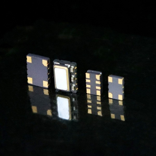
Frequency: 74.25MHz
Supply Voltage: 1.8V
Frequency Stability: ±30ppm
Output Type: LVDS
Operating Temperature Range: -40~85℃
The 74.25MHz LVDS Differential Crystal Oscillator is a high-performance clock source designed for demanding high-speed data applications. Featuring a compact 2520 SMD package (2.5x2.0mm) and operating at a low voltage of 1.8V, this oscillator delivers exceptional frequency stability (±30ppm) and ultra-low phase jitter of only 0.5ps rms.
The LVDS (Low Voltage Differential Signaling) output ensures high noise immunity and low electromagnetic interference (EMI), making it perfect for high-definition video processing and optical communication modules. Engineered for reliability, it operates across an industrial temperature range from -40°C to +85°C.
Target Frequency: 74.250000 MHz (Optimized for HD Video/HDMI).
Output Type: LVDS Differential output for high-speed integrity.
Ultra-Low Jitter: 0.5ps rms (12kHz to 20MHz) for clean signal transmission.
Miniature Footprint: 2.5 x 2.0 x 1.1 mm (max) SMD package.
Industrial Grade: Reliable operation from -40°C to +85°C.
Power Efficiency: 1.8V supply voltage with Standby function (OE).
Video Systems: HDTV, Camera, HDMI/DisplayPort interfaces.
Networking: Gigabit Ethernet, Fiber Channel, SONET/SDH.
Computing: High-speed FPGA and SoC clocking, PCIe storage.
Item | Parameters | Condition | Electrical Specifications | |||
MIN | TYP | MAX | UNITS | |||
1 | Nominal Frequency (Fo) | 74.250000 | MHz | |||
2 | Oscillation Mode | FOD | ||||
3 | Operating Temperature | -40 | - | 85 | ℃ | |
4 | Storage Temperature | -55 | - | 125 | ℃ | |
5 | Frequency Stability | Note 1 | -30 | - | 30 | PPM |
6 | Supply Voltage | 1.71 | 1.8 | 1.89 | V | |
7 | Current Consumption | RL=100Ω | - | - | 40 | mA |
8 | Standby Function | Internal Pull Up | YES | |||
9 | Current Consumption(Standby) | OE=Low | - | - | 30 | uA |
10 | Output Type | LVDS | ||||
11 | Output Load | 100 | Ω | |||
12 | Output Voltage High | - | 1.43 | 1.6 | V | |
13 | Output Voltage Low | 0.9 | 1.1 | - | V | |
14 | Offset Voltage | 1.125 | 1.250 | 1.375 | V | |
15 | Differential Output Voltage | 247 | 330 | 454 | mV | |
16 | Rise Time | 20% ~ 80% Output Swing | - | - | 0.5 | nS |
17 | Fall Time | 80% ~ 20% Output Swing | - | - | 0.5 | nS |
18 | Symmetry | 45 | 50 | 55 | % | |
19 | Start-up Time | To 90% of Final Amplitude | - | - | 50 | mS |
20 | Enable Voltage High (Logic 1) | Note 2 | 0.7VDD | - | - | V |
21 | Enable Voltage Low (Logic 0) | Note 2 | - | - | 0.3VDD | V |
22 | Output Enable Delay Time | - | - | 2 | mS | |
23 | Output Disable Delay Time | - | - | 200 | nS | |
24 | Phase Jitter | 12K ~ 20MHz | - | - | 0.5 | pS rms |
Note 1: Inclusive of frequency tolerance at 25degC, variation over temperature, supply voltage variation, aging and vibration.
Note 2: Output will be enable if OE is Logic 1 or open ; Output will be disable if OE is Logic 0.
Note 3: The standard testing environment except temperature test is 25±5degC, 40%~70% relative humidity.
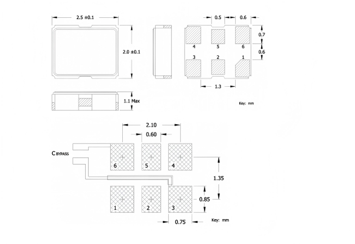
| PIN | FUNCTION |
| 1 | OE |
| 2 | NC |
| 3 | GND |
| 4 | OUT |
| 5 | OUT |
| 6 | VDD |
Contact: Katya Vane
Phone: +86-18884136031
Tel: +86-28-80192520
Email: sales@xtalong.com
Add: No.4 of XinHang Road, West of High-tech zone, Chengdu City 611731, China
We chat