Email: sales@xtalong.com Tel: +86-28-80192520
Email: sales@xtalong.com Tel: +86-28-80192520
1. Frequency: 10MHz (±0.01 ppb accuracy).
2. Holdover: < 1us timing error / 24h.
3. Phase Noise: -155 dBc/Hz (@10kHz).
4. Power: 3.3V (400mA steady state).
5. Interface: 1PPS In/Out + UART.
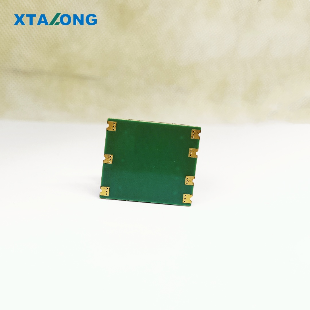
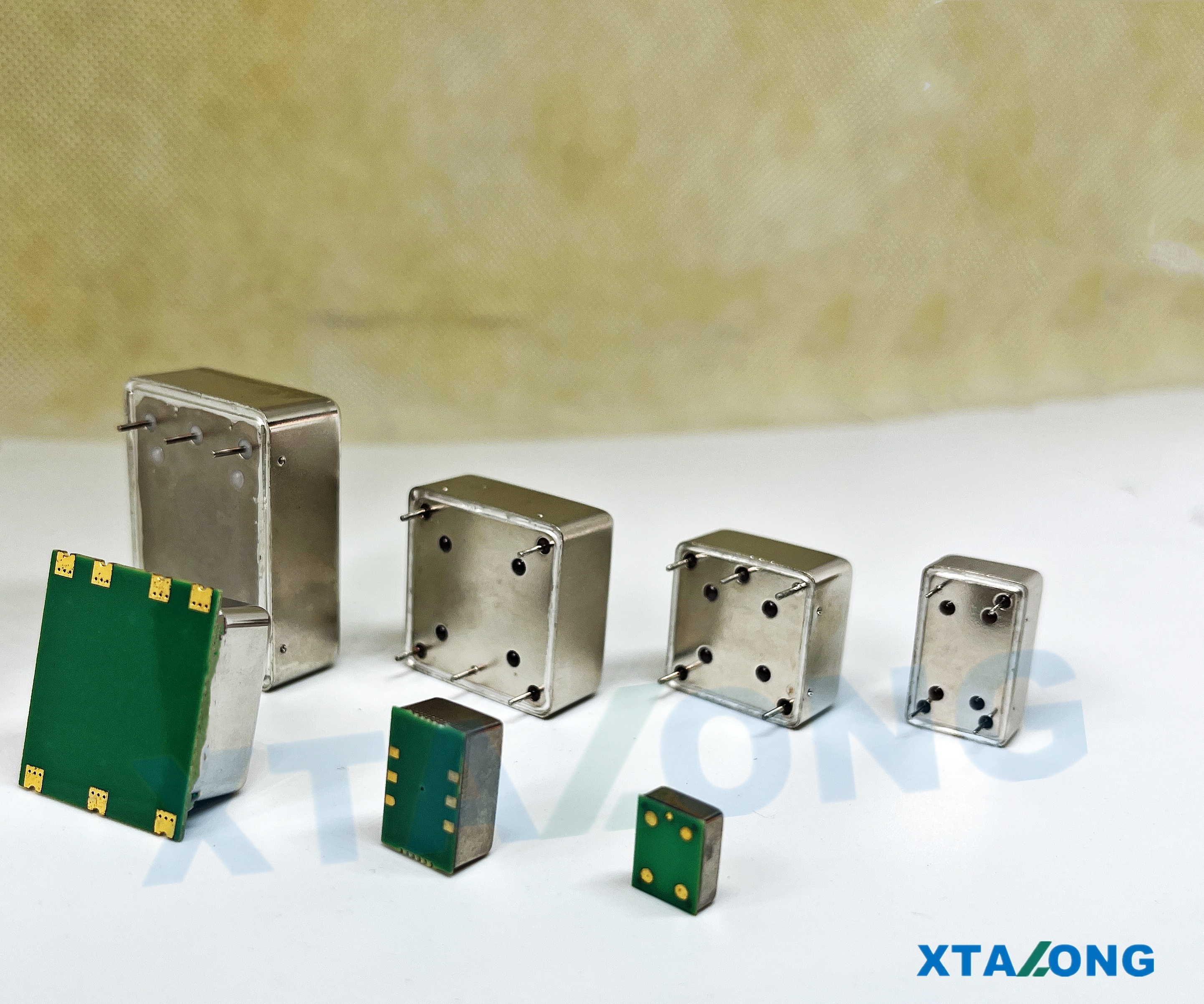
A high-precision 10MHz GNSS-disciplined clock module with 1PPS synchronization and 3.3V supply.
| Parameter | Min. | Typ. | Max. | Unit | Condition | Note | ||
|---|---|---|---|---|---|---|---|---|
| Frequency Stability (Pin 4) | Frequency | 10 | MHz | |||||
| Frequency Accuracy | -100 | +100 | ppb | Free run, @25℃, after 15mins power on ref to nominal frequency | ||||
| -0.01 | +0.01 | ppb | The average value within 24 hours after deep locked to GNSS | |||||
| Reflow shift | -100 | +100 | ppb | place for 72 hours after reflow,and power up for 30 minutes | Internal frequency components must be allowed to rest for 72 hours following high-temperature processing. | |||
| Short Term Stability | 0.01 | ppb/s | After power on 1hour@Free run | |||||
| Temperature Stability | -1 | +1 | ppb | -10℃~+65℃ refer to 25℃ | ||||
| Holdover Capability | -1 | +1 | us | ΔT=2℃,locking to 1PPS from GNSS for 7days, measure the holdover for 24 hours, with the ΔT less than 1℃/h. | ||||
| Local 1PPS precision | -30 | +30 | ns | Refer to 1PPS from GNSS for 24 hours | ||||
| Aging | Per day | -0.5 | +0.5 | ppb | After 30days of operation @Free run | |||
| the first year | -50 | +50 | ppb | |||||
| Supply Voltage/Current(pin3) | Voltage Supply | 3.135 | 3.3 | 3.465 | V | |||
| Operating Current | 1200 | mA | During warm up | |||||
| 400 | mA | At steady state operation @25℃ | ||||||
| RF Output (pin4) | LVCMOS | Load | 15 | pF | ||||
| High Level (VoH) | 2.7 | V | ||||||
| Low Level (VoL) | 0.4 | V | ||||||
| Rise/Fall Time | 5 | ns | ||||||
| Duty Cycle | 45 | 55 | % | |||||
| RF Phase Noise(pin4) | Phase Noise | -85 | dBc/Hz | @1Hz | ||||
| -118 | @10Hz | |||||||
| -140 | @100Hz | |||||||
| -150 | @1kHz | |||||||
| -155 | @10KHz | |||||||
| 1pps Output(pin2) | LVCMOS | Output Level(VOH) | 2.7 | V | ||||
| Output Level(VOL) | 0.4 | V | ||||||
| Pulse width | 100 | ms | ||||||
| 1pps Reference Input(pin1) | LVCMOS | Input Level(VOH) | 2.7 | 3.4 | V | |||
| Input Level(VOL) | 0 | 0.4 | V | |||||
| Pulse width | 0.01 | 500 | ms | |||||
| RXD(pin5) | LVCMOS | Input Level(VOH) | 2.7 | V | ||||
| Input Level(VOL) | 0.4 | V | ||||||
| TXD(pin6) | LVCMOS | Input Level(VOH) | 2.7 | V | ||||
| Input Level(VOL) | 0.4 | V | ||||||

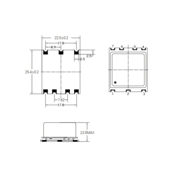
| Pin Definition | |||
| Number | PIN | Function | |
| 1 | Reference 1pps In | 1 PPS Reference Input | |
| 2 | 1pps Out | Local 1PPS Output | |
| 3 | VS | Supply voltage: 3.3 V | |
| 4 | RF out | Frequency Output: 10 MHz | |
| 5 | RXD | Serial ReceptionSerial Reception | 115200-N-8-1 |
| 6 | TXD | Serial Transmission | |
| 7 | GND | GND | |
Contact: Katya Vane
Phone: +86-18884136031
Tel: +86-28-80192520
Email: sales@xtalong.com
Add: No.4 of XinHang Road, West of High-tech zone, Chengdu City 611731, China
We chat